In view of the increasing requirements from industry and on the part of end users, the selective protection of electronic components is becoming more and more important. With regard to simple electrical insulation and protection against corrosion, in many cases a thin film coating may be adequate. However, additional challenges, such as vibration protection and protection against the influences of extreme weather can make the complete potting of components necessary.
The dam-and-fill concept offers a compromise between these two possibilities and combines the advantages of both methods in that it constitutes a thick film coating. Figure 1 illustrates the different possibilities for protection.
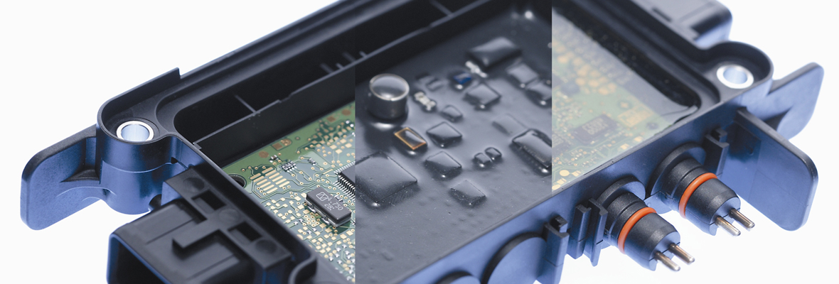
Here, the boundaries between the different methods of protection are not clearly defined. Layer thicknesses of less than 100 µm are usually described as thin layer coatings, up to 300 µm as thick layer coatings, and above this as potting.
With the dam-and-fill concept it is possible to obtain layer thicknesses from 100 µm up to 2 mm, so that we can speak of either a thick film coating or a thin layer potting. With this type of electronic protection it is not only possible to protect the sensitive components against corrosion, but also against mechanical influences and aggressive chemicals. The essential advantage compared with complete potting is the potential material savings.
The method
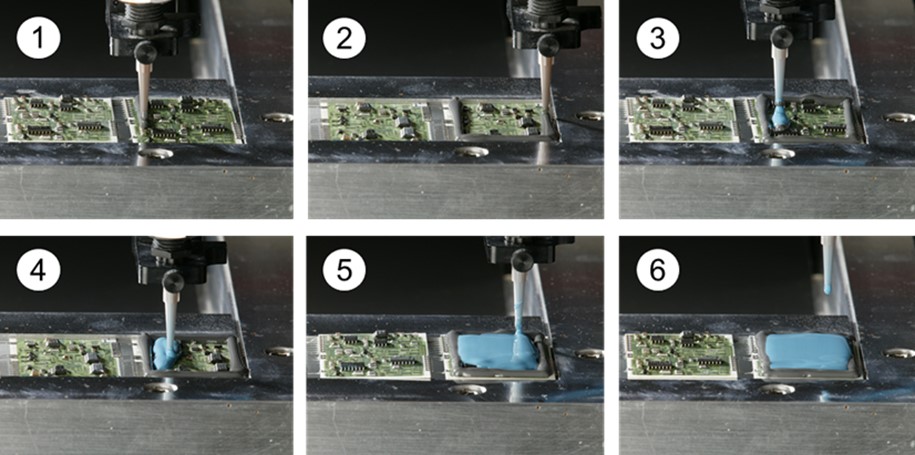
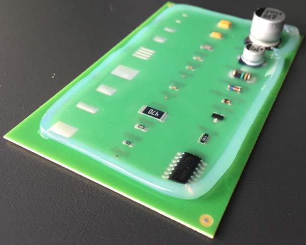
Dam-and-fill is a selective process enabling the protection of selected components on the printed circuit board without influencing neighboring regions.
Two materials with different viscosities are used. A high viscosity material is first applied as a dam around the region to be protected. The resulting pit is then filled with a low viscosity material until this covers all components or up to the desired height. Figure 2 shows detailed photos of the individual steps of the method.
Typically, we can obtain layer thicknesses of up to 1 mm. For special applications, higher layer thicknesses may be required, since some components would otherwise not be adequately protected or, in the worst case, not be coated at all. In this case, it may be necessary to apply two dams over one another in order to obtain a higher dam (see Figure 3).
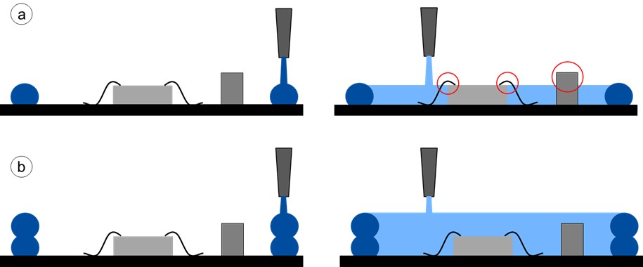
Here, the placing of the dam is an important step that enormously influences the final result of the thin layer potting. The high viscosity dam material forms the barrier that fixes the low viscosity filler material in the selected regions of the printed circuit board. Accordingly, the application of the dam with uniform height and without voids is extremely important, since the filler material can otherwise leak out.
Rheology of the dam material
The rheology of the dam material is an important quality criterion for the shaping of the dam. The viscosity of the dam materials ranges from about 30,000 to 1,300,000 mPa·s. However, the transport through the pump or pressing out of a cartridge causes shearing of the material, frequently resulting in decreasing viscosity. In order to prevent the dam from running while impinging on the printed circuit board the rapid restoration of the viscosity is of essential importance. This behavior, also called thixotropy, is achieved with special filler materials and is what makes a dam-and-fill application possible at all.
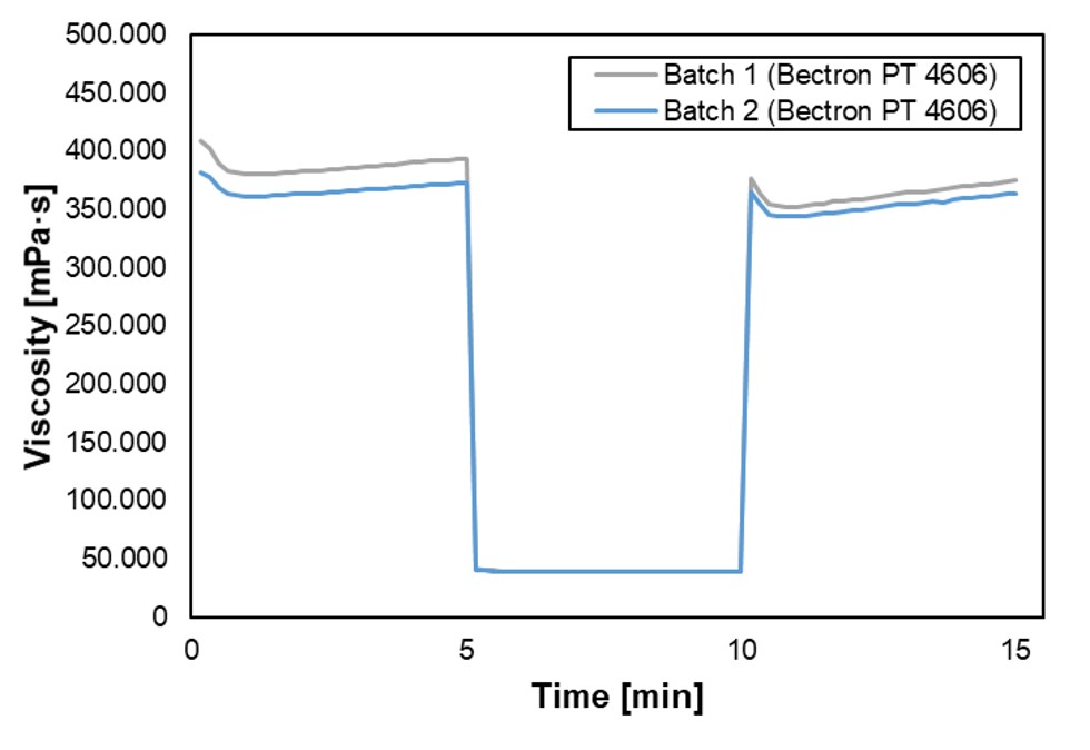
Figure 4 shows the thixotropic behavior for the example of two charges of Bectron® PT 4606. In phase 1 of the measurement, the material is subjected to a very low shear rate (γ=0.5 s-1 ). In the second phase, the shear rate is abruptly increased (γ=12.5 s-1
 ) in order to simulate pressing out of the cartridge or dispensing head. It can be seen that the viscosity decreases due to the increase in the shear rate. This shear-diluting behavior favors the material transport on the one hand, but at the same time the material would then impinge on the printed circuit board with such a low viscosity that it can no longer form a dam. The rapid restoration of the viscosity is consequently necessary during the reduction of the shear rate, as can be seen in phase 3. For a reduction of the shear rate to γ=0.5 s-1 the viscosity again increases abruptly, preventing the running of the dam.
Specially developed ELANTAS products
Because of the diverse possibilities for applications the demand for products with the dam-and-fill method is continually rising. ELANTAS Europe already recognized the potential of this method many years ago and developed special products for this application. This resulted in product lines with different properties that offer a tailor-made solution for different cases of applications.
Bectron PT product line:
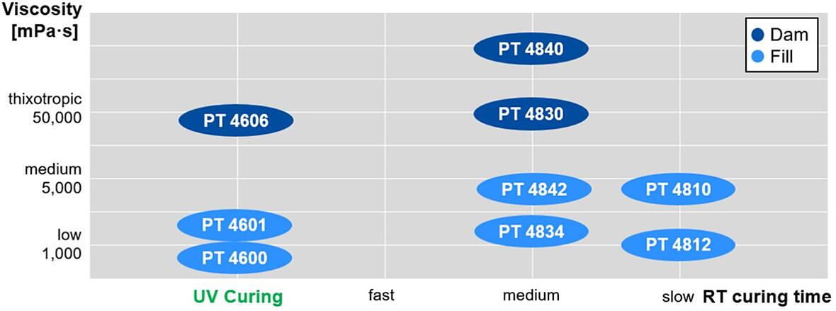
The Bectron® PT product line comprises single-component polyurethane/acrylate chemistry UV and/or moisture cross linking materials. The products possess good adhesion on many surfaces and exhibit convincing behavior under thermal shock from -40° to +120 C. According to application case and requirement, the customer can choose between materials with different curing methods. Bectron® PT 46xx are products that harden either through UV radiation or by reacting with atmospheric humidity. Curing by UV radiation thereby serves as a fast curing mechanism, producing a stable material within a few seconds that can be further processed directly. However, at the same time PT 46xx products are characterized by a second curing mechanism that functions by reaction with atmospheric moisture and ensures curing in the shadowed regions under the components. This mechanism is much slower and, for a 3 mm layer thickness, requires two or three days 23°C and 50 % relative humidity. Bectron® PT 48xx products are very similar in terms of their chemistry and their properties. The difference lies in the curing process. The Bectron® PT 48xx product line hardens only by reacting with atmospheric moisture. Moisture curing is however significantly faster than for the PT 46xx product line. Under the same conditions, the surface is already tack-free five or six hours after application, so that further processing is possible. Complete curing takes about 24 hours. Figure 5 gives an overview of the currently available Bectron® PT products, classified according to viscosity, curing mechanism and time.
Bectron PK product line:
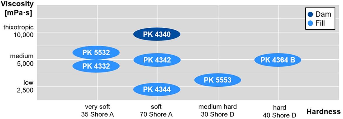
The Bectron® PK product line also comprises single-component polyurethane systems that harden thermally. The special feature of the PK products is that the hardener is premixed in encapsulated form with the resin and subsequently released by the influence of temperature. This unique technology avoids problems with incorrect mixing proportions and makes complicated system technology for mixing the resin and hardener unnecessary. Bectron® PK materials are solvent free and have a low glass transition temperature. Furthermore, they exhibit good properties under thermal shock from -50 to +125 °C. Depending on the requirements, a variety of PK products with different material hardnesses and viscosities exists. Figure 6 shows a selection of these.
Silcones:
In addition to the single-component polyurethanes, ELANTAS Europe also offers single-component silicones for use as a dam-and-fill combination. A material combination shown also in Figure 7 consists of Bectron® SA 70P1-30 (dam material) and Bectron® SC 76V1-20 (filler material). Both materials are condensation cross-linked. During the reaction with access to atmospheric humidity, methanol is split off (so-called alkoxy cross-linking). The primary advantages of this silicone material combination are the high thermal stability and the marked flexibility over the entire range of operating temperatures (-50° to +200°C).
Summary
Dam-and-fill is a precise process in which the combination of a high viscosity dam material and a low viscosity filler material enables the selective protection of electronic components on the printed circuit board. The resulting thin layer potting offers significantly better protection than conventional thin layer varnish. At the same time, compared with complete potting, with the selective process it is possible to eliminate the housing and save substantial amounts of potting material otherwise required.
Did we catch your interest?
Do not hesitate to contact us under bectron.elantas.europe@altana.com and ask for a free sample.
Learn more about our portfolio for electronic protection.
Materials for Electronic Protection (elantas.com)